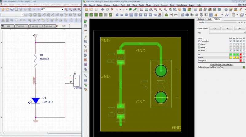
Starting with OrCAD and Cadence Allegro PCB – Tutorial for Beginners
For everyone who would like to learn how to start with OrCad and Cadence Allegro.
CHAPTERS:
00:00 – Introduction: What you are going to learn
02:35 – Starting a new project
03:56 – Creating Resistor Symbol
06:01 – Creating LED Symbol
08:35 – Creating Connector Symbol
09:19 – Creating Through hole pad
11:35 – Creating SMD pad
13:18 – Creating VIA
14:19 – Creating Resistor Footprint
16:12 – Creating Footprint for LED
17:31 – Creating Connector Footprint
18:54 – Assign footprints to symbols
19:57 – Placing components and Drawing Schematic
23:14 – Annotating Schematic
24:28 – How to update symbol ans sync schematic
26:55 – Generating Netlist
27:48 – Starting New PCB
29:10 – Placing components in PCB
31:10 – Creating Board Outline
32:11 – Setting up Rules
34:45 – Doing Layout
37:36 – Adding Text
40:39 – Moving tracks and placing components on the bottom layer
41:48 – Working with Layers and Views
47:16 – How to sync changes in PADs and Footprints with PCB
52:25 – Adjusting LED Footprint
56:11 – Checking DRC and Generating Gerbers
1:00:10 – Generating Drill File
1:01:19 – Printing Layers
1:02:20 – Generating BOM, Printing Schematic
Would you like to support me in what I do? It’s simple:
– sign up for one of our Schematic and PCB Design online courses at http://www.fedevel.com/academy/
– support me through Patreon page https://www.patreon.com/robertferanec
– sign up for my Udemy courses: https://www.udemy.com/user/robertferanec/
Or:
– send me an email and/or leave a positive comment
– watch and like the videos 🙂
– read my Welldone Blog at http://www.fedevel.com/welldoneblog/
– spread a word about FEDEVEL Academy
It is much appreciated.
– Robert
atoll logiciel


